Article – The Future of CMOS is Stacked
11th September 2023
Custom stacked CMOS sensors will add new performance and features in a tiny package
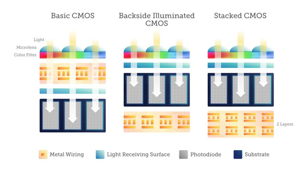
In December 2021, Sony Semiconductor Solutions announced a breakthrough at the IEEE International Electron Devices Meeting with a new stacked CMOS image sensor technology. Where conventional CMOS image sensors place photodiodes and pixel transistors on the same plane, this new technology separated photodiodes and pixel transistors onto different substrate layers. This new approach promised wider dynamic range and reduced noise.
While notable, this was one more step in a technology that has been developing for decades. And now sensor manufacturers are starting to really explore the possibilities of this stacked design approach. Yole Intelligence is predicting that after a transitional period in 2022, the CMOS image sensor (CIS) market will return to steady growth, reaching $29 billion dollars in 2028. The company sees custom CIS products for more niche, lower-volume differentiated markets, as a key driver for the overall market. Stacked CMOS design opens up many more opportunities for CMOS chips that are designed for specific applications and creating new kinds of competitive advantage.
“We are now at a point where manufacturing processes that were fundamentally experimental 20 years ago are becoming within reach of commercial applications,” explains Rafael Romay-Juarez, the Executive VP and General Manager at Teledyne Imaging Machine Vision Sensors. “This is just the start of a more transformational opportunity, where 3D stacked sensors are an opportunity to bring more added-value functionality into CMOS image sensors in a cost-effective manner.”
Read the full article here.